Legacy Products
5x86 Processor Brief
NOTE: The information provided below is for a Cyrix product that is no longer in production.
 The
5x86™ processor utilizes efficient fifth-generation architectural
features to significantly improve performance while minimizing
transistor count. It achieves this performance using a superpipelined
architecture in the integer unit combined with data forwarding, branch
prediction, a 16-KByte unified write-back cache, single-cycle
instruction decode, and single-cycle execution. The processor's
built-in power-saving features automatically power down the Floating
Point Unit (FPU) and other idle internal circuits, while the System
Management Mode (SMM) conserves power flowing to system peripherals. The
5x86™ processor utilizes efficient fifth-generation architectural
features to significantly improve performance while minimizing
transistor count. It achieves this performance using a superpipelined
architecture in the integer unit combined with data forwarding, branch
prediction, a 16-KByte unified write-back cache, single-cycle
instruction decode, and single-cycle execution. The processor's
built-in power-saving features automatically power down the Floating
Point Unit (FPU) and other idle internal circuits, while the System
Management Mode (SMM) conserves power flowing to system peripherals.
 Features and Benefits Features and Benefits
The Cyrix 5x86™ processor,
formerly called the M1sc, is first in a family of processors for
desktop and mobile systems. With its fifth-generation architectural
core, the 5x86 processor gives users an affordable performance
alternative to the Pentium® processor with a market-ready socket
solution.
Fifth-Generation Architecture
The new 5x86 processor family rivals the performance of Pentium®
processors to achieve compelling system performance while consuming
only half the power of competing alternatives. Fifth-generation
architectural features were carefully evaluated and selected for their
contribution toward maximum efficiency, performance, and simplicity of
design. Features such as a 64-bit internal architecture, branch
prediction, data forwarding, and multiple operations issued per clock
(made possible by a decoupled load/store unit) are combined with an
80-bit floating point unit (FPU) and 16K unified write-back cache.
Aggressive power management features conserve power within the
processor as well as power flowing to system peripherals.
Minimal Power Consumption
The Cyrix 5x86 architecture was engineered with power-saving
intelligence to track, monitor, and automatically power down the
floating point unit and other internal circuits when not in use. It
features Cyrix's proven system management mode (SMM) to control power
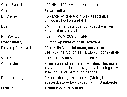
flowing to system peripherals. At 100 MHz @ 3.3 volts, the 5x86
processor consumes less than 3.5 watts of power, which minimizes heat
dissipation and makes the 5x86 processor the ideal choice for
power-sensitive mobile systems.
Package
The Cyrix 5x86 processor is an example of Cyrix's strategy to design
next-generation processor architectures that leverage existing designs.
It is initially available in a 168-pin PGA or a 208-pin QFP package.
This socket solution offers easy design-in with minimal board space
requirements for maximum integration flexibility.
| Features and Benefits | Architectural Overview | Technical Specifications |
| Performance Benchmarks | Page Top |
Architectural Overview
In designing the Cyrix 5x86
processor, Cyrix engineers analyzed the performance features of the M1
processor. The goal was to identify those features that could increase
the performance of a single-execution pipeline with minimum added
transistor count and power consumption.
Two facts were fundamental in
identifying features for the 5x86: the 32-bit architectural standard of
x86 technology, and the average instruction length for existing
8/16-bit and 32-bit code. These facts enabled Cyrix to reduce the bus
width required to handle most data and code transactions to 32 bits. To
exploit the inherent parallelism, the 5x86 utilizes decoupled units
interconnected with multiple 32-bit, split-transaction buses.
The 5x86 processor employs a
dedicated branch unit including a branch target buffer, a 16-KByte
unified write-back cache, a Floating Point Unit, and an instruction
fetch and instruction decode unit. The Memory Management Unit contains
a 32-entry translation lookaside buffer, a load/store unit capable of
managing concurrent operations, and an address calculation unit. The
5x86 functional units are interconnected by two 32-bit buses that
permit non-blocking operation of the units. A 128-bit instruction fetch
bus feeds 16 bytes of code per cycle to a three-line-deep buffer in the
instruction decode unit.
Integer Unit
The superpipelined Integer Unit fetches, decodes, and executes x86 instructions through the use of a six-stage integer pipeline.
- The Instruction Fetch Stage
generates a continuous, high-speed instruction stream from the on-chip
cache. Up to 128 bits of code are read during a single clock cycle.
- The Instruction Decode Stage evaluates the code stream
provided by the instruction fetch stage and determines the number of
bytes in each instruction and the instruction type. Instructions are
processed and decoded at a maximum rate of one instruction per clock.
- The Address Calculation function is superpipelined to contain
two stages -- AC1 and AC2. If the instruction refers to a memory
operand, AC1 calculates a linear memory address for the instruction.
AC2 performs any required memory management functions, cache accesses,
and register file accesses. If a floating point instruction is
detected, AC2 sends it to the FPU for processing.
- The Execution Stage, under control of microcode, executes
instructions using the operands provided by the address calculation
stage.
- Write-Back updates the register file within the integer unit,
or writes to the load/store unit within the Memory Management Unit.
Floating Point Unit (FPU)
The
5x86 FPU is based on the same core as that found in Cyrix's
sixth-generation M1 processor. The FPU interfaces with the integer unit
and the cache unit through a 64-bit interface. It is x87
instruction-set compatible (including the extended 80-bit format) and
adheres to the IEEE-754 standard. Since most applications contain FPU
instructions mixed with integer instructions, the 5x86 achieves high
performance by completing integer and FPU operations in parallel.
Write-Back Cache
The 5x86 implements a 16-KByte, four-way set associative unified
instruction/data cache that can operate in either write-back or
write-through mode. It has a dedicated 128-bit port for transferring
instructions to the IF unit, and a 64-bit wide data port that can be
split into two 32-bit data paths. The cache is arranged as four sets of
256 lines per set with 16 bytes per line. Cache buffers allow an entire
cache line to be read or written in a single clock cycle to maximize
cache bandwidth. Since the 5x86 is scalar and implements these buffers,
it alleviates the need for more sophisticated cache banking techniques
for concurrent accesses.
Memory Management Unit (MMU)
The 5x86 MMU contains the load/store unit, the 32-entry translation
lookaside buffer (TLB), and the address calculation (AC) unit. The AC
unit performs all address calculations, maintains instruction pointers
for each pipeline stage, and initiates load and store transfers. The
advanced load/store unit is capable of managing concurrent operations
and processing loads and stores out of order while maintaining a
three-deep load queue and four-deep store queue.
The Bus Interface Unit
The 5x86 64-bit internal bus is tapered down to a 32-bit external bus
to allow the processor to fit existing designs, a strategy that
minimizes customers' development cycles. The 5x86/100 MHz core speed
option can operate with a bus speed of either 33 MHz or 50 MHz. The 120
MHz core speed option operates with a bus speed of 40 MHz. Eight
buffers allow sufficient buffering of write activity to maintain
bandwidth for read operations, thus reducing pipeline stalls. The bus
protocol is standard except for an optional higher-performance linear
burst mode, which can be implemented instead of the Cyrix
"one-plus-four" mode. The one-plus-four mode is compatible with all
existing 32-bit chipsets.
Power Management
The 5x86 was engineered with advanced power management features. The
processor monitors and automatically powers down the FPU and other idle
internal circuits. Each 32-bit section of the 64-bit internal data bus
is driven only when needed. The core design of the 5x86 is completely
static to allow for easy clock manipulation, a feature commonly used to
adjust processor power consumption. Additionally, the System Management
Mode (SMM) software model implemented is compatible with past and
future Cyrix processors and can be used to perform processor and system
power conservation tactics.
| Features and Benefits | Architectural Overview | Technical Specifications |
| Performance Benchmarks | Page Top |
Technical Specifications
| Features and Benefits | Architectural Overview | Technical Specifications |
| Performance Benchmarks | Page Top |
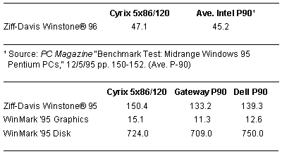
Cyrix 5x86/120 Performance Benchmarks*
System-Level Performance Results
Windows®-based benchmarks execute scripts that run actual Windows
applications such as word processing, desktop publishing, database
management, computer-aided design (CAD), and scientific/engineering
(MathCAD) software. These benchmarks generally weight the results of
each application (based on the application's unit market share) and
derive a composite performance score.
Processor-Intensive Performance Results
DOS-based benchmarks illustrate 32-bit and 16-bit performance of the
Cyrix 5x86 processor. Some of these benchmarks are small enough to fit
in the 16-KByte on-chip cache, avoiding any dependency on the design or
the second-level cache. CPUmark16
is a large-format benchmark that does not fit in the internal cache. It
demonstrates the performance of the combined CPU and memory subsystem,
including the external second-level cache.
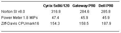
*System Configurations
Cyrix reference systems: 120 MHz 5x86 CPU, Chicony 471A or ECS
UP 8810-AIO Motherboard, 16MB DRAM, 256K L2 cache, Diamond Stealth VLB
- Chicony Platform and Diamond Stealth 64 PCI - ECS platform, 64-bit
VRAM, Conner CFA 540A, 524MB hard disk, IDE (on board I/F). Windows for
WorkGroups 3.11, 20MB SWAP file, 32 bit file and disk access.
Gateway P90: 90 MHz Pentium® processor, 16MB DRAM, no L2 cache,
Diamond Stealth 64 PCI, 2MB VRAM, Conner CFA540A IDE, 524MB hard disk,
10ms access time, on board PCI IDE. Windows for WorkGroups 3.11, 20MB
SWAP file, 32 bit file and disk access.
Dell P90: 90 MHz Pentium® processor, 16MB DRAM, 256K L2 cache,
Number Nine PCI, Conner CFA540A IDE, 524MB hard disk, 10ms access time,
on board PCI IDE. Windows for WorkGroups 3.11, 20MB SWAP file, 32 bit
file and disk access.
Pentium® is a registered trademark of Intel Corporation. All other
brand or product names are trademarks or registered trademarks of their
respective holders.
Cyrix 5x86/100 Performance Benchmarks*
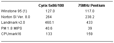
*All systems tested with 256K L2 cache.
(1) All systems tested with identical hard drive and graphics card.
|